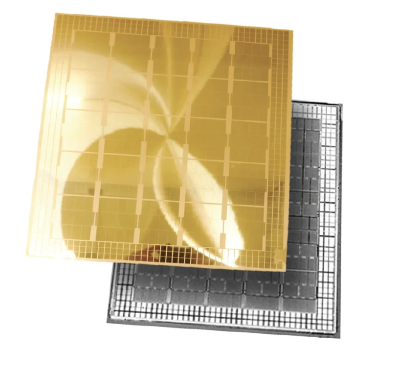
Supports higher throughput, reduced cycle time, and lower cost per package, while enabling integration of increasingly complex multi-die architectures. The post Automated 310mm Panel-Level Packaging to Accelerate AI Innovation: Tech Brief appeared first on Semiconductor Engineeri
Supports higher throughput, reduced cycle time, and lower cost per package, while enabling integration of increasingly complex multi-die architectures. The post Automated 310mm Panel-Level Packaging to Accelerate AI Innovation: Tech Brief appeared first on Semiconductor Engineering .
Source: Semiconductor Engineering — read the full report at the original publisher.
This is a curated wire item. The Continuum Brief does not republish full third-party articles; this entry links to the original source.