Automated 310mm Panel-Level Packaging to Accelerate AI Innovation: Tech Brief
Supports higher throughput, reduced cycle time, and lower cost per package, while enabling integration of increasingly complex multi-die architectures. The post Automated 310mm Panel-Level Packaging to Accelerate AI Innovation: Tech Brief appeared first on Semiconductor Engineering .
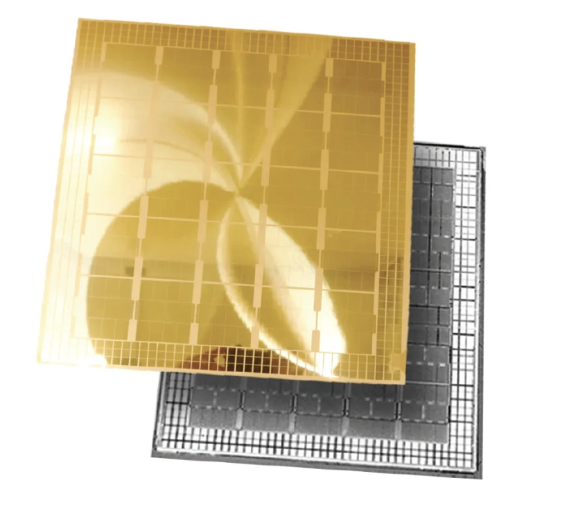
The increasing demand for AI compute necessitates more efficient and cost-effective packaging solutions, pushing panel-level packaging technologies into the spotlight.
Advanced packaging is a critical bottleneck and enabler for AI innovation, directly influencing performance, cost, and design flexibility of next-generation AI hardware.
The adoption of larger panel-level packaging formats changes the economics and throughput of advanced semiconductor manufacturing, facilitating denser and more complex multi-die architectures.
- · Advanced packaging equipment manufacturers
- · AI hardware developers
- · Semiconductor manufacturers with advanced packaging capabilities
- · Cloud AI service providers
- · Traditional packaging methods
- · Semiconductor companies without advanced packaging R&D
Higher performance and lower cost AI accelerators become more accessible due to manufacturing efficiencies.
Increased competition in the AI chip market as design and production barriers are lowered for complex multi-die systems.
New AI applications become viable due to the combination of powerful and economically produced hardware, accelerating the AI innovation cycle.
This signal links to a primary source. Continuum Brief monitors and indexes it as part of the live intelligence stream — we do not republish source content.
Read at Semiconductor Engineering