Chinese university builds 3D chip design tool tailored to Huawei's ‘LogicFolding’ architecture — 3D design delivers increased performance and better thermal management
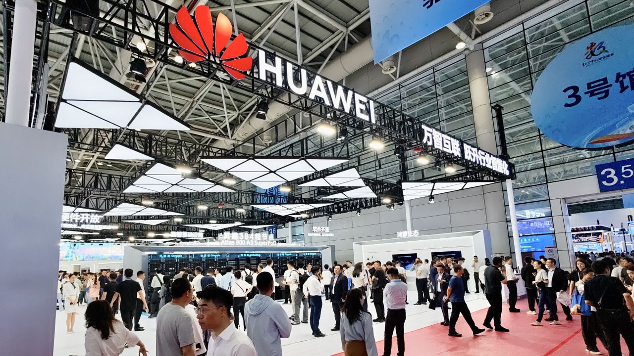
The announcement came two days after Huawei presented LogicFolding and its accompanying Tau Scaling Law at ISCAS 2026.
China is aggressively pursuing semiconductor self-sufficiency and advanced computing solutions due to ongoing geopolitical tensions and export controls.
This development indicates a significant leap in China's domestic chip design capabilities, potentially reducing reliance on foreign intellectual property and tools for advanced packaging.
China now possesses a bespoke chip design tool for 3D stacking, offering competitive performance and thermal advantages, tailored to specific domestic architectures like Huawei's LogicFolding.
- · Huawei
- · Chinese semiconductor industry
- · Domestic IP developers
- · US EDA tool vendors
- · Foreign chip design software providers
Huawei gains a significant advantage in developing high-performance, efficiently packaged chips for its systems.
This encourages other Chinese firms to invest further in domestic EDA tools and advanced packaging technologies, accelerating indigenous innovation.
The global semiconductor supply chain becomes more bifurcated, with distinct Chinese and non-Chinese ecosystems for advanced chip design and manufacturing.
This signal links to a primary source. Continuum Brief monitors and indexes it as part of the live intelligence stream — we do not republish source content.
Read at Tom's Hardware