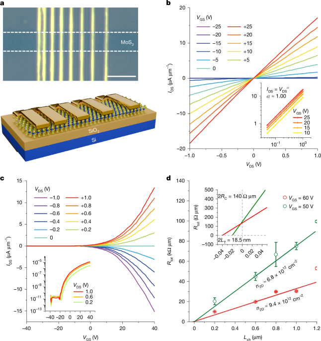
Nature, Published online: 01 July 2026; doi:10.1038/s41586-026-10707-0 Cross-sectional scanning tunnelling microscopy shows a 2 nm carrier transfer length in bismuth-contacted monolayer MoS2 transistors, defining metal-contact scaling limits for sub-10 nm 2D electronic devices.
Advances in understanding material properties at the nanoscale are enabling breakthroughs previously limited by characterization techniques.
This research provides a fundamental understanding of critical limitations for future transistor scaling, directly impacting the roadmap for advanced semiconductor devices.
The identified 2 nm carrier transfer length sets a new benchmark for metal-contact scaling, suggesting new engineering challenges and opportunities for sub-10 nm 2D electronic devices.
- · 2D material researchers
- · Semiconductor foundries
- · High-performance computing sector
- · Incumbent silicon chip manufacturers (without 2D material adoption)
- · Companies relying on traditional scaling methodologies
The finding will accelerate research and development into optimizing contacts for 2D material transistors, critical for future node development.
Improved transistor performance from 2D materials could lead to more energy-efficient and powerful integrated circuits, impacting various technology sectors.
The ability to scale transistors further might extend Moore's Law well beyond current predictions, driving a new era of computational power and miniaturization.
This signal links to a primary source. Continuum Brief monitors and indexes it as part of the live intelligence stream — we do not republish source content.
Read at Nature — Latest Research