Post-silicon era gets closer as industry giants crack the 2D transistor scaling bottleneck with breakthrough tech — imec, ASML, and TSMC fab complementary 2D-material transistors at 50nm pitch on a 300mm wafer
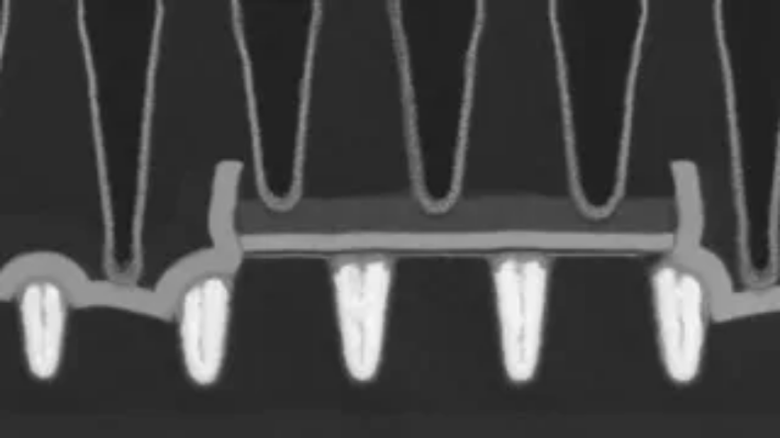
Imec, ASML, and TSMC have integrated both n-type and p-type transistors with atomically thin 2D channels on a single 300mm wafer.
The semiconductor industry is aggressively pursuing solutions to overcome the physical limits of silicon-based transistors, making breakthroughs in 2D material scalability highly timely.
This breakthrough extends the roadmap for advanced semiconductor manufacturing, directly impacting future compute capabilities and the economic and geopolitical balance of power in tech.
The ability to fabricate 2D material transistors at 50nm pitch on 300mm wafers means the 'post-silicon era' is closer to commercial viability, offering pathways to denser and more energy-efficient chips.
- · ASML
- · TSMC
- · Imec
- · AI/HPC sector
- · Legacy chip architectures
- · Semiconductor companies without advanced R&D
Further acceleration in chip density and performance, enabling more powerful computing devices and AI systems.
Increased pressure on global supply chains for advanced materials and manufacturing equipment required for 2D transistor production.
Potential for new killer applications in edge AI and specialized computing, previously limited by power or size constraints.
This signal links to a primary source. Continuum Brief monitors and indexes it as part of the live intelligence stream — we do not republish source content.
Read at Tom's Hardware