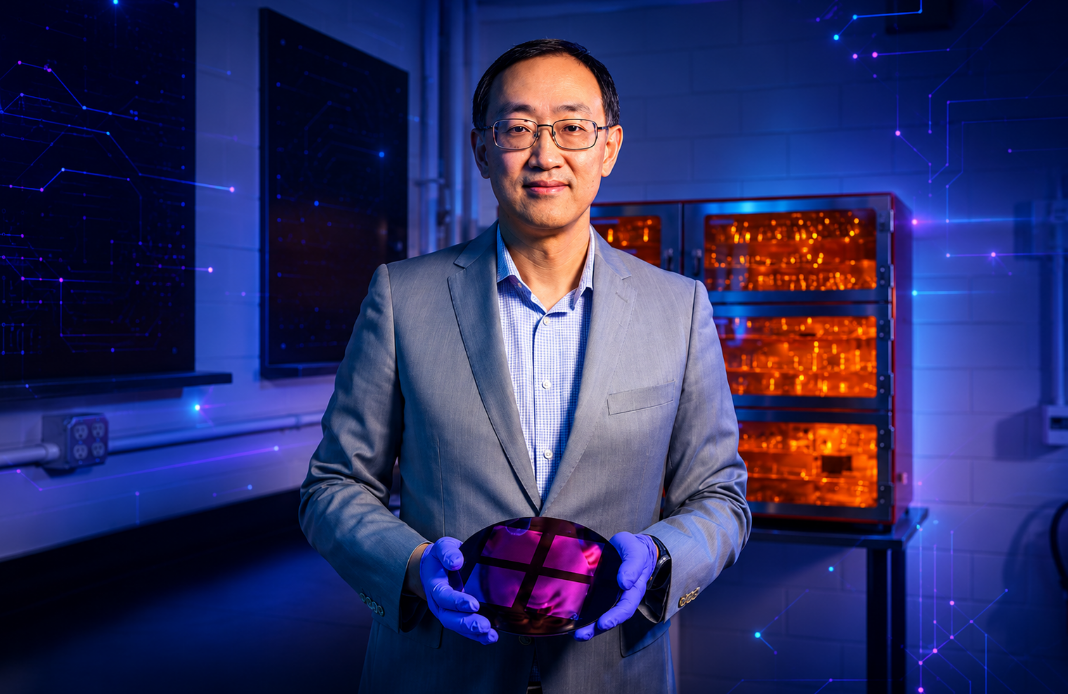
Insider Brief PRESS RELEASE — Researchers led by Illinois Grainger Engineering professor Qing Cao have demonstrated a scalable way to directly and sequentially stack high-performance silicon circuits. This advance marks a critical step toward realizing the full potential of three-dimensional chips that could carry computing beyond the limits of traditional scaling. For more than half […]
Advances in materials science and manufacturing techniques are reaching a point where complex 3D semiconductor integration is becoming viable, driven by the relentless demand for higher performance and density.
This breakthrough addresses fundamental physical limits of traditional chip design, potentially enabling future computing capabilities essential for AI and advanced applications.
The ability to sequentially stack high-performance silicon circuits in a monolithic fashion changes the paradigm of chip design from predominantly 2D to truly 3D, enhancing density and reducing interconnects.
- · Semiconductor manufacturers
- · High-performance computing sector
- · AI hardware developers
- · University of Illinois
- · Companies reliant solely on planar scaling
- · Less innovative chip design firms
Increased transistor density and improved power efficiency in advanced processors.
Accelerated development of AI models and applications due to more powerful and efficient compute.
Potentially democratized access to high-performance computing capabilities, fostering innovation across various industries.
This signal links to a primary source. Continuum Brief monitors and indexes it as part of the live intelligence stream — we do not republish source content.
Read at The Quantum Insider